
At a glance
- 01 Why Is Traditional EUV’s Resolution Insufficient?
- 02 What Is High-NA? What Has Changed?
- 03 What Technical Challenges Does High-NA Bring?
- 1. Larger Lens Volume → More Complex Optical Path
- 2. Major Mask Design Overhaul → Narrower Image Field
- 3. Greater Sensitivity to Imaging Errors
- 4. Amplified Mask Defects
- 5. Doubled Light Source Brightness Required
- 04 What Does ASML’s High-NA EUV Machine Look Like?
- 05 Can High-NA Directly Etch <2nm Chips?
- 06 High-NA’s Significance Goes Beyond "Line Width"
- 07 Mass Production Timeline: When Will It Enter Your Smartphone?
- 08 The Door to 0.5nm Is Opening
Core improvements of High-NA: Traditional EUV has a numerical aperture (NA) of 0.33, while High-NA EUV features an NA of 0.55.
The smartphone chip you use today may already employ EUV lithography technology, with key process nodes breaking through to 3nm.
But this is far from enough.
In scenarios like artificial intelligence, high-performance computing, and AR/VR, chips are approaching physical limits.
Traditional EUV lithography is hitting resolution bottlenecks as it attempts to further shrink line widths.
The door to overcoming this bottleneck is being opened by next-generation technology: High-NA EUV (High Numerical Aperture Extreme Ultraviolet Lithography).
Without changing the light source wavelength, it expands imaging precision from the original 13nm to 8nm, 5nm, and even 2nm.
Can this technological leap truly take us into the 0.5nm manufacturing era?
In this article, we uncover the secrets of High-NA EUV.
01 Why Is Traditional EUV’s Resolution Insufficient?
Let’s first review a formula:
Rayleigh’s Law of Lithography Resolution:Resolution = k1 * λ / NA
Where:
- Resolution: The lithography resolution.
- λ: Light source wavelength (fixed at 13.5nm for traditional EUV).
- NA: Numerical Aperture, describing the system’s light-gathering capability.
- k1: Process factor, influenced by process optimization, computational lithography, immersion, etc., with a theoretical minimum of approximately 0.25.
In traditional EUV systems: NA ≈ 0.33.
Thus, even with λ = 13.5nm, resolution is limited to around 13~16nm.
However, key chip dimensions (such as metal line widths) have long been smaller than this level, requiring complex processes like Double/Quad Patterning, offset compensation, and etch repair.
This severely slows production efficiency and increases defect rates.
02 What Is High-NA? What Has Changed?
Core improvements of High-NA:
- Traditional EUV: Numerical Aperture NA = 0.33
- High-NA EUV: NA = 0.55
- Resolution improvement ratio: Traditional 1×, High-NA ~1.7×
- Minimum line width: Traditional EUV ~13nm, High-NA EUV ~8nm (theoretically down to 5nm)
Fundamental change: The optical system is more "light-concentrated."
Definition of Numerical Aperture (NA):NA = n * sin(θ)
Where:
- n: Refractive index of the light propagation medium (fixed at 1 in EUV, as it operates in a vacuum).
- θ: Maximum angle of incidence.
The only way to increase NA is to focus light more "obliquely"—i.e., expand the angle at which the system accepts light.
This brings revolutionary changes to mirror design, optical paths, and mask structures.
03 What Technical Challenges Does High-NA Bring?
1. Larger Lens Volume → More Complex Optical Path
NA = 0.55 means a steeper light slope, requiring much larger projection lens assemblies.The system’s optical path must be redesigned with an asymmetric optical layout (annular field).
2. Major Mask Design Overhaul → Narrower Image Field
The projection field of view is reduced, making it impossible to expose the entire pattern in one pass."Stitching" (mosaic-style exposure) must be used.The mask size is reduced to an asymmetric 6×9mm area, posing challenges for pattern consistency.
3. Greater Sensitivity to Imaging Errors
Higher NA → Shallow depth of field → Increased demand for focusing precision.Overlay (layer alignment) error requirements are pressed below 2nm.Wafer surface unevenness, thermal expansion/contraction, and stage precision all face new challenges.
4. Amplified Mask Defects
Larger incident angles make mask defects "more prominent."Stronger Mask Defect Inspection and compensation mechanisms are mandatory.
5. Doubled Light Source Brightness Required
High-NA systems collect light at a wider angle → but the light aperture is smaller, reducing light intensity.Thus, the EUV light source needs to be upgraded from 250W to ≥500W.
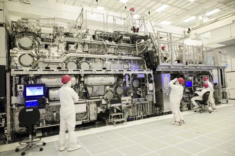
04 What Does ASML’s High-NA EUV Machine Look Like?
ASML’s newly launched High-NA system is named: EXE:5000 Series
Key features include:
- Total lens assembly weight > 6 tons.
- Equipped with a brand-new Zeiss optical system, featuring more lenses and special-shaped designs.
- Supports 0.55 NA and high-precision stitching exposure.
- Compatible with 500W+ light sources (supplied by Trumpf + Cymer).
- Overall height > 4 meters, occupying an area larger than 2 shipping containers!
05 Can High-NA Directly Etch <2nm Chips?
Theoretically, it can etch feature line widths down to 5nm or even 2nm.Resolution = 13.5 / (2 * 0.55) = 12.3nm; with process factor k1 < 0.3, further shrinking is possible.
The key lies in supporting technologies such as computational lithography (OPC), mask correction, and resist performance.
Its main goal is not "narrower lines," but "simpler processes."
Current 3nm chips often require 3~4 exposures to complete. High-NA’s target is to finish major layers in one exposure!
This means: simpler chip processes, higher exposure yields, shorter lithography cycles, and (theoretically) lower chip costs.
06 High-NA’s Significance Goes Beyond "Line Width"
It represents a restructuring of the entire lithography machine architecture:
- Precision upgrade: Entering the era of <1nm alignment error.
- Intelligent control systems: AI-powered parameter tuning for system stability.
- Process simplification: Reduced multi-patterning → cost reduction and yield improvement.
- Greater defect sensitivity: Spurring the industrial chain for higher-precision mask inspection and repair.
- Stronger light sources: Accelerating the further evolution of EUV light source technology.
07 Mass Production Timeline: When Will It Enter Your Smartphone?
- 2023: ASML completed assembly of EXE:5000 prototypes.
- 2024: Customer testing (Intel as the first customer).
- 2025: Small-batch trial production (Intel’s 18A node).
- 2026: Potential for commercial mass production (processes below 3nm).
- 2027+: Gradual popularization in high-end smartphones/AI chips.
The first manufacturers to adopt High-NA are almost all pursuers of extreme performance:
- Intel: Emphasizing leading-node manufacturing, betting on High-NA to reclaim technological leadership.
- ASML: As the sole supplier, targeting large-scale shipments by 2030.
- TSMC / Samsung: More cautious but with simultaneous evaluation and deployment plans.
08 The Door to 0.5nm Is Opening
High-NA EUV is the most revolutionary lithography leap since EUV itself.
It represents:
- Technology shifting from "pushing limits" to "breaking bottlenecks."
- Processes moving from "compensating for errors" to "system optimization."
- Chip manufacturing transitioning from "manual stitching" to "optical limit control."
Every exposure is precise to the arrangement of atoms;Every wafer is the symphony of optics and control systems.
We are still some distance from the 0.5nm era, but High-NA has already opened the door to that future.